1. Why can an AI chip finish millions of simple math sums so fast?
2. What fun job were GPUs originally built to speed up before scientists used them for AI?
🤯 Mind-Blowing Fact • Grade 2
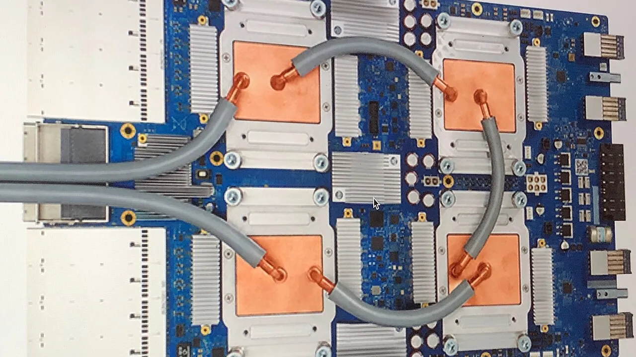
Top AI chips work so hard doing trillions of calculations per second that data centers often cool them with chilled liquid flowing through copper plates!
✨ Word Sparks (Grade 2 Glossary)
Tap 🔊 to hear
GPU
Graphics chip with thousands of parallel cores
TPU
Custom chip built specially for AI math
neural network
Computer program inspired by connected brain cells
🪝
How did video-game graphics cards accidentally launch the modern age of artificial intelligence?
1
One Boss vs. An Army
Every laptop has a main brain called a CPU that acts like a clever head chef solving tricky recipes step by step. Yet when millions of tiny multiplication problems pile up at once, even the fastest single chef falls behind!
2
From Video Games to Brain Models
In 1999, engineers introduced the —short for Graphics Processing Unit—packed with hundreds of small calculators to shade 3D game triangles all at once. Around 2012, AI researchers realized needed that exact same grid math!
3
Custom Chips Built for AI
In 2015, Google engineers designed the —Tensor Processing Unit—from scratch purely for . Today, and TPUs help doctors spot tiny X-ray clues, fold proteins, and power helpful AI assistants.
1. How is a GPU or TPU different from a computer's traditional CPU?
2. Why do giant data centers often run cool water through metal plates on top of AI chips?
🤯 Mind-Blowing Fact • Grade 3
The word 'systolic' in a TPU's systolic array comes from the medical word for your heart's rhythmic pumping beat—because data pulses step by step across thousands of math cells in lockstep!
✨ Word Sparks (Grade 3 Glossary)
Tap 🔊 to hear
matrix
Rectangular grid of numbers arranged in rows
systolic array
Grid pulsing data rhythmically between math units
transistor
Microscopic electronic switch etched onto silicon
🪝
What do lighting a 3D dragon's scales in a video game and teaching an AI to recognize puppies have in common?
1
Surprise! It's All Grid Math
Zoom in on a 3D video game character spinning on screen: to figure out where every point moves and how light bounces off every triangle, the chip multiplies huge tables of numbers called matrices. Amazingly, artificial neural networks learn by multiplying giant number tables, too!
2
The 2012 Deep Learning Spark
After Nvidia launched programmable GPUs in 1999 and opened them to science code with CUDA in 2006, three researchers trained a neural network named AlexNet on two bedroom gaming GPUs in 2012. AlexNet crushed world image-recognition records overnight!
3
Heartbeat Grids Inside TPUs
Moving numbers back and forth to memory wastes energy. So in 2015, architect Norm Jouppi's team built Google's Tensor Processing Unit around a ''—a square grid that pumps numbers rhythmically from neighbor to neighbor like blood from a beating heart!
4
Powering Science Discovery
Linked by ultra-fast optical fibers in supercomputers, modern AI accelerators forecast hurricanes days earlier, map galaxies, and predict 3D shapes of life-saving medicine molecules.
1. Why did 3D video-game GPUs turn out to be ideal for training neural networks in 2012?
2. Why is the grid inside a TPU called a 'systolic' array?
🤯 Mind-Blowing Fact • Grade 4
Moving two numbers from external memory onto a silicon chip burns more than 100 times as much electrical energy as actually multiplying those two numbers together!
✨ Word Sparks (Grade 4 Glossary)
Tap 🔊 to hear
Multiply-Accumulate
Multiplying two numbers and adding to total
High-Bandwidth Memory
Vertically stacked memory chips feeding data ultra-fast
throughput
Total amount of work finished per second
🪝
Why is shuttling data two centimeters across silicon more expensive than doing the actual math—and how do AI chips beat the 'Memory Wall'?
1
Multiply-Accumulate: The Atom of AI
Peek inside any modern neural network—from voice assistants to protein-folding models—and over ninety percent of its workload boils down to one humble arithmetic step repeated quadrillions of times: multiply an input number by a connection weight, and add it to a running sum (, or MAC).
2
Breaking Past Sequential Bottlenecks
Traditional CPUs devote most of their silicon area to giant caches and branch predictors so complex single-threaded programs never stall. By contrast, Nvidia's GPU evolution (1999 GeForce 256, 2006 CUDA, and 2017 Tensor Cores) and Google's 2015 TPU strip away complex control circuitry to tile tens of thousands of compact ALUs across the die.
3
Beating the Memory Wall With HBM and Smart Precision
Surprisingly, fetching a number from off-chip DRAM consumes over a hundred times more energy than multiplying it! AI chips attack this 'Memory Wall' in two ways: stacking skyscrapers of (HBM) right beside the processor on a silicon interposer, and shrinking 32-bit decimals down to nimble 16-bit (`BF16`) or 8-bit formats that quadruple without hurting accuracy.
4
Edge NPUs In Your Pocket
Not every AI chip lives in a warehouse: miniature Neural Processing Units (NPUs) tucked inside smartphones and hearing aids run speech recognition and camera enhancements locally using less than two watts of battery power!
1. What consumes the most electrical energy inside modern computing hardware if engineers aren't careful?
2. How does switching neural network math from bulky 32-bit numbers to compact 16-bit or 8-bit numbers help AI chips?
🤯 Mind-Blowing Fact • Grade 5
One modern AI accelerator executing 4 petaFLOPS performs as many math operations in a single second as a human doing one calculation every second would finish in 126 million years!
✨ Word Sparks (Grade 5 Glossary)
Tap 🔊 to hear
tensor
Multi-dimensional array holding numbers for AI math
petaFLOPS
One quadrillion math operations finished per second
quantization
Representing weights with compact, lower-bit numbers
🪝
How do 100-billion-transistor chips etched with extreme ultraviolet light execute quadrillions of tensor operations every second?
1
Beyond Von Neumann Sequential Computing
For seventy years, classical computer architecture followed John von Neumann's blueprint: a central processing unit fetching instructions one by one across a shared memory bus. Deep neural networks shattered that paradigm—demanding trillions of simultaneous linear-algebra operations (Y = W · X + B) across multi-dimensional arrays known mathematically as .
2
SIMT GPUs and Domain-Specific Systolic TPUs
Two complementary silicon architectures rose to meet that demand. Modern GPUs employ Single-Instruction, Multiple-Thread (SIMT) streaming multiprocessors augmented with dedicated matrix Cores, descended from Nvidia's 1999 GPU and 2006 CUDA platform that powered AlexNet's historic 2012 ImageNet breakthrough. Taking specialization further in 2015, Norm Jouppi and colleagues unveiled Google's TPU around huge 128×128 or 256×256 2D systolic arrays (inspired by H. T. Kung and Charles Leiserson's 1978 theory), holding neural weights stationary inside MAC cells while streaming activations across without touching SRAM registers.
3
Numerical Formats, Photolithography, and 3D Packaging
Etched at 3-nanometer feature scales using Extreme Ultraviolet (EUV) lithography, flagship AI accelerators pack over 100 billion transistors onto reticle-limit dies. Utilizing Brain Floating Point (`BF16`), `FP8`, and `INT4` , a single accelerator delivers multiple (10¹⁵ operations per second), fed at several terabytes per second through thousands of microscopic silicon-interposer wires connected to 3D-stacked High-Bandwidth Memory (HBM).
4
Optical Interconnects and Warehouse-Scale Superpods
Training frontier foundation models exceeds any single chip's memory, so engineers network tens of thousands of GPUs or TPUs into unified 'pods' via multi-hundred-gigabit copper and optical circuit-switched interconnects—coordinating distributed gradients across entire rooms as one giant logical supercomputer.
5
Neuromorphic and Photonic Horizons
To curb megawatt data-center power budgets, chip architects now explore analog in-memory resistive crossbars, spiking neuromorphic processors modeled on biological synapses, and silicon-photonic waveguides that multiply matrices at the literal speed of laser light.